QuNP

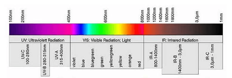
Quantum Nanophotonics LLC ( QuNP ) is currently developing new cutting edge advanced technology for a new generation of VIS - NIR - SWIR - MWIR - LWIR Photodetectors and Imaging Array Sensors based on Quantum NanoPhotonics.
The "Quantum NanoPhotonics" Advanced Product Innovation Design Center in our Irvine-CA HQ has secured several "Pending Patents" with USPTO and it is seeking active collaboration with Photonics Research Institutes and Industry Partners to engage in a Joint Venture for prototyping of next generation Photonics products and commercialization of its disruptive technology.
Contact us for more details and inquiries for your specific Advanced Photodetector product development needs.
Specializing in:
Custom High Reliability Photonics/Optoelectronic Product Development
Photodetector Sensors & Imaging PD Arrays (UV,Visible, NIR, SWIR)
Nanoporous-Si NIR Enhanced Detectors
Heterostructure Broadband VIS-NIR-SWIR-MWIR-LWIR Photodetetcors
Si PIN QUAD Fast Response NIR Detectors
Lateral and Dual Axis PSDs (Position Sensitive Diodes)
Radiation Hard Detectors (High Reliability & Space Applications)
X-Ray Detector Array Imaging (Medical & Security Applications)
SOI and Epi based UltraFast Detectors
Phototransistors
NPI (New Product Introduction) Commercialization:
- Raw Materials: High Resistivity FZ-Si, HP-Si
- Advanced Materials for NanoPhotonics
- Supply Chain support for Photonics R&D Prototyping:
- Photonics Processing Development
- Process Flow Integration
- Mask IC Design & GDSII
-Subcontracting Specialized Process Services:
Ion Implantation:
Dose Range: 1e11 to 1e16
Energy Range: 5KeV to 1MeV
PECVD Si3N4(Low Stress): 250Å-10,000Å
Sputtering Metallization: Most Metals&Alloys
E-Beam Metallization: Most Metals
Mask Making: Laser Direct Write
Turn Key Wafer Fab Foundries, Test & Assembly:
Si Wafer Fab Foundry
III-V Wafer Fab Foundry
NanoFabrication & MEMS
Wafer Test Facilities
Assembly Facilities
Analytical Service Facilities
Transfer to Pilot Line Manufacturing with Subcontracted Foundries
Process Flow Mapping
Yield Enhancements
Total Quality Management evaluation, 6s, FMEA, PFMEA, CA, CI
Lean Manufacturing 6s-Plus
Technology Capability Evaluation
Process Equipment Technology Evaluation & Selection
IP Evaluation
Value Chain Management
Executive Business Management support for Small Business / Start-Ups
Technical Support with Business Acquisition/Divestiture transition


